Other Research Areas in the Group
Scan-distortion & Hysteresis Diagnosis and Correction
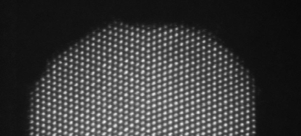
Modern electron microscopes are able to deliver deep sub-angstrom resolution, however in scanned systems the precision in positioning of the electron probe becomes increasingly important. The group researches methods to observe, diagnose and compensate errors in probe-scanning to deliver images with the highest possible precision.
Photogrammetry on the Microscale for 3D Surface Imaging in the SEM
The scanning electron microscope (SEM) is a powerful imaging tool. Its many different detectors produce a variety of 2D images offering a wealth of information about a specimen. Unfortunately, the SEM yields its data as 2D images of our 3D samples. Alternative techniques could be applied to obtain true topological information, such as atomic force microscopy (AFM), but what if the sample is too rough for these techniques?
Photogrammetry is a technology which yields 3D maps of objects by combining 2D images taken from multiple viewing angles. Increased interest in Drone photography as lead to a wave of new low-cost photogrammetry software packages that were previously only available to archaeologists and conservators.
This research area will evaluate these new software tools for their compatibility with SEM image data to deliver 3D metrology at the nano-scale. This approach has not been attempted before and if successful could yield a powerful new tool for the analysis of 3D printed object surface-quality, biological imaging, and information-technology metrology.
Reduced Energy-spread Electron Emitters
The electron emitter is the start of the entire electron imaging process. When examining materials at low voltages in a Transmission electron microscope (TEM), if the energy spread of electron emitter is large it can greatly degrade the image resolution. This is particularly problematic when examining nanomaterials and biological materials which might require low voltages to avoid damage to the sample.
Since the creation of the thermionic electron emitter many new technologies have emerged over the years to reduce the energy spread of the electrons, from the invention of the cold field-emission gun to the creation of electron monochromators. However, these technologies can be very costly to the consumer.
This project seeks to understand the opportunities for producing electron emitters with intrinsically lower energy spreads to improve low-voltage imaging without the use of expensive electron monochromator technology. Prototypes of a low-cost low energy spread electron emitter are currently being developed using multi-physics modelling software. The next stage of the project will involve making a physical prototype of the electron emitter and running experiments to test it limits and improve its performance and design.
Thermal Management
This work aims to investigate the electrical stability and thermal-management of electron-lenses to improve performance and increase sustainability.
Evaluation of Additive Manufacturing (3D Printing) for Electron Microscopy
This research theme seeks to identify potential opportunities with, and risks for, using 3D printing in the manufacture of EM equipment and accessories.


/filters:quality(100)/prod01/channel_3/media/tcd/physics/research-groups/ultramicroscopy/images/banners/det.png)
/filters:quality(100)/prod01/channel_3/media/tcd/physics/research-groups/ultramicroscopy/images/banners/7.png)
/filters:quality(100)/prod01/channel_3/media/tcd/physics/research-groups/ultramicroscopy/images/banners/2100-thermal-881X497.jpg)