Scanning Tunneling Microscopy
Our STM research can be summarized into three main areas;
- Metal oxides; Single crystalline [7,9] and ultra-thin film metal oxides [4,5,8,13,15,17]. The ultra-thin films are synthesized by oxidising a metal single crystal.
- 2D materials; Transition Metal Dichalcogenides [1,2], Few-layer graphene synthesized on silicon carbide [6,11], fullerene monolayers (for example C60) [12,13,17] and ultra-thin film metal oxides.
- Nano-scale structures; Metal and metal oxide clusters [4,8,18] and nano-scale defects in crystalline materials.
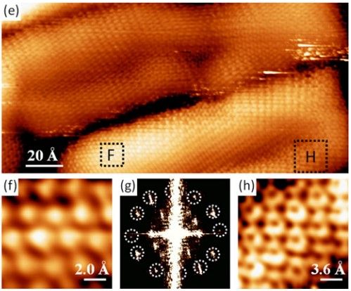
Below are some selected STM images;


Current STM researchers
- Kuanysh Zhussupbekov
- Sam Berman
Selected STM publications
- Zhussupbekov, Kuanysh, et al. "Electronic and structural characterisation of polycrystalline platinum disulfide thin films." RSC Advances 10.69 (2020): 42001-42007.
- K. Zhussupbekov, L. Ansari et al. “Imaging and identification of point defects in PtTe2” npj 2D Materials and Applications 5. 1 (2021)
- Frolov, Alexander S., et al. "Atomic and Electronic Structure of a Multidomain GeTe Crystal." ACS nano 14.12 (2020): 16576-16589.
https://pubs.acs.org/doi/abs/10.1021/acsnano.0c05851 - Kuanysh, Zhussupbekov, et al. "Oxidation of Nb (110): atomic structure of the NbO layer and its influence on further oxidation." Scientific Reports (Nature Publisher Group) 10.1 (2020). https://search.proquest.com/openview/c100f674ce05d10798c4ec2dd5609d52/1?pq-origsite=gscholar&cbl=2041939
- Bozhko, Sergey I., et al. "Surface modification on MoO 2+ x/Mo (110) induced by a local electric potential." Scientific reports 9.1 (2019): 1-11. https://www.nature.com/articles/s41598-019-42536-9
- Aristov, Victor Yu, et al. "Layer-by-layer graphene growth on β-SiC/Si (001)." ACS nano 13.1 (2018): 526-535. https://pubs.acs.org/doi/abs/10.1021/acsnano.8b07237
- Walls, B., et al. "Reflectance anisotropy spectroscopy of Fe 3 O 4 (110): Anisotropic strain." Physical Review B 98.4 (2018): 045428. https://journals.aps.org/prb/abstract/10.1103/PhysRevB.98.045428
- Lübben, O., et al. "Nanoclusters and nanolines: the effect of molybdenum oxide substrate stoichiometry on iron self-assembly." Nanotechnology 28.20 (2017): 205602.
https://iopscience.iop.org/article/10.1088/1361-6528/aa6b50/meta - Walls, B., et al. "Oxygen vacancy induced surface stabilization:(110) terminated magnetite." Physical Review B 94.16 (2016): 165424. https://journals.aps.org/prb/abstract/10.1103/PhysRevB.94.165424
- Bozhko, Sergey I., et al. "Composite Fe3O4–W (100) probes for scanning tunneling microscopy." Journal of Applied Physics 122.23 (2017): 235301.
https://aip.scitation.org/doi/abs/10.1063/1.5001057 - Chaika, Alexander N., et al. "Rotated domain network in graphene on cubic-SiC (001)." Nanotechnology 25.13 (2014): 135605.
https://iopscience.iop.org/article/10.1088/0957-4484/25/13/135605/meta - Murphy, Barry E., et al. "Homolytic cleavage of molecular oxygen by manganese porphyrins supported on Ag (111)." ACS nano 8.5 (2014): 5190-5198.
https://pubs.acs.org/doi/abs/10.1021/nn501240j - Bozhko, S. I., et al. "Disclinations in C 60 molecular layers on WO 2/W (110) surfaces." Physical Review B 90.21 (2014): 214106.
https://journals.aps.org/prb/abstract/10.1103/PhysRevB.90.214106 - Chaika, A. N., et al. "High resolution STM imaging with oriented single crystalline tips." Applied surface science 267 (2013): 219-223.
https://www.sciencedirect.com/science/article/abs/pii/S0169433212019265 - Krasnikov, Sergey A., et al. "Writing with atoms: Oxygen adatoms on the MoO 2/Mo (110) surface." Nano Research 6.12 (2013): 929-937.
https://link.springer.com/article/10.1007%252Fs12274-013-0370-2 - Chaika, A. N., et al. "Control of the spatial resolution in ultimately high resolution STM experiments with [001]-oriented single crystalline tungsten probes." Physics Procedia 32 (2012): 785-788.
https://www.sciencedirect.com/science/article/pii/S187538921201053X - Bozhko, Sergey I., et al. "Rotational transitions in a C 60 monolayer on the WO 2/W (110) surface." Physical Review B 84.19 (2011): 195412.
https://journals.aps.org/prb/abstract/10.1103/PhysRevB.84.195412 - Lübben, Olaf, et al. "Fe nanoclusters on the Ge (001) surface studied by scanning tunneling microscopy, density functional theory calculations and X-ray magnetic circular dichroism." Nano Research 4.10 (2011): 971.
https://link.springer.com/article/10.1007%252Fs12274-011-0153-6 - Lübben, Olaf, et al. "Self-assembly of Fe nanocluster arrays on templated surfaces." Journal of Applied Physics 111.7 (2012): 07B515.
https://aip.scitation.org/doi/abs/10.1063/1.3676207