Nanoscience breakthrough puts low-cost, printable electronics on the horizon
Posted on: 05 December 2025
The breakthrough has a huge potential impact – one that brings us much closer to quickly and cheaply producing printable electronics such as wearable health sensors or flexible displays. The scientists have solved a long-standing mystery governing the way layered materials behave, which has yielded a universal, predictive framework for the future of the 2D semiconductor industry.
Imagine wearable health sensors, smart packaging, flexible displays, or disposable IoT controllers all manufactured like printed newspapers. The same technology could underpin communication circuits, sensors, and signal-processing components made entirely from solution-processed 2D materials.
But until now, finding and developing the 2D materials that could enable such devices was largely trial and error.
We hadn’t known why some layered materials “electrochemically exfoliate” into nanosheets while others fail completely. Electrochemical exfoliation uses an electrical current to force ions into the layers of a bulk material, weakening the forces that hold them in shape, and causing the material to form thin, 2D nanosheets, if successful – some of which have myriad uses.
“Because there has never been the means to predict which materials will behave like this, and produce nanosheets with the properties we need to unlock various applications, only a handful of 2D materials have ever been processed into networks of printed 2D transistors,” said Dr Tian Carey, a newly appointed Royal Society–Research Ireland Research Assistant Professor from Trinity College Dublin’s School of Physics and AMBER, the Research Ireland Centre for Advanced Materials and BioEngineering Research.
“Here, we’ve shown that we can unlock dozens of new 2D semiconductors. We’ve already fabricated state-of-the-art printed transistors with over 10 new materials, unlocking new circuits for the first time. these include printed digital-to-analogue converters and BASK communication circuits, which are capable of encoding digital messages into high-frequency signals – the fundamental building blocks of modern computing.”
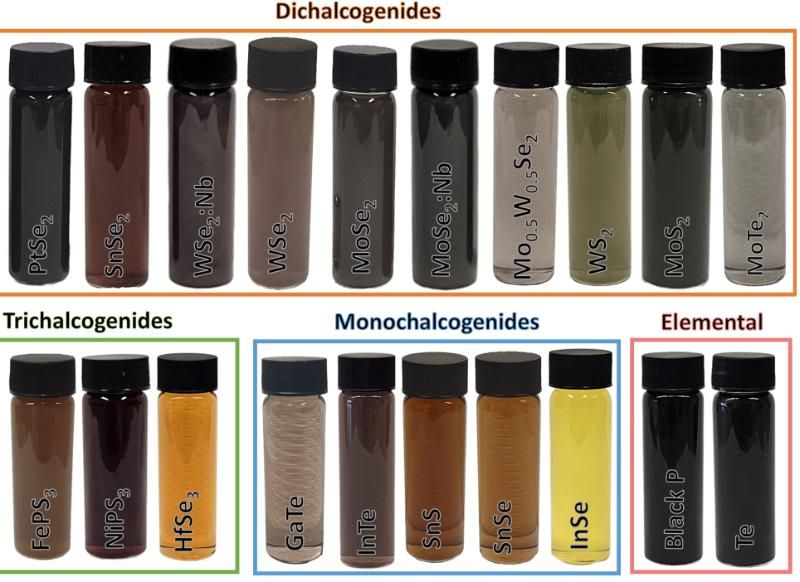 Some brightly coloured semiconducting and metallic inks produced as part of this work led by Dr Tian Carey. Image: Dr Tian Carey.
The key seemingly lies in ensuring “in-plane stiffness” is higher than out-of-plane stiffness. This represents a measure of how resistant the material is to deformation when put under pressure from different perspectives (in-place being along the material; out-of-plane being perpendicular).
The research, led by Dr Tian Carey, in collaboration with Prof. Jonathan Coleman and colleagues, now has a predictive framework pinpointing the stiffness thresholds required for successful exfoliation across many different materials.
Using this, they created high-aspect-ratio nanosheet inks and built working transistors and circuits from them, including the first printed DACs and communication circuits.
Dr Carey added: “It’s very exciting to imagine a new wave of electronic innovations, all of which could be manufactured like printed newspapers one day in the future. In theory, this approach could yield abundant low-cost, flexible, and high-performance 2D electronics.”
“We now also understand from this work that each transistor's performance is limited by junctions between semiconductors rather than by defects within the semiconductors themselves, which is important in helping us direct future efforts. With this in mind, our next step will be to reduce the impact of these ‘flake-to-flake’ junctions to unlock the next big performance jump.”
Other collaborating institutions on this work include Politecnico di Milano, TU Delft, EPFL, and UCT Prague. The project received funding from the European Union’s Horizon Europe research and innovation programme, for example via the HYPERSONIC project awarded to Prof. Coleman, AMBER; via a Marie Skłodowska-Curie Individual Fellowship (project MOVE); and a Royal Society-Research Ireland University Research Fellowship (project THINK).
The recently published journal articles can be read on the Nature Communications website.
Dr Carey recently secured a prestigious Royal Society University Research Fellowship (URF) to build an independent research group in Trinity. You can read more about this in this dedicated spotlight feature on the Trinity News & Events pages.
URFs, awarded to outstanding scientists in the early stages of their research careers, and to those with the potential to become leaders in their fields, provide salary costs and research expenses for up to eight years.
Dr Carey will now grow his team and lead a project that will develop printed electronics using two-dimensional (2D) materials – specifically field-effect transistors (FETs) and circuits, which make up some of the fundamental building blocks of modern computing.
Media Contact:
Thomas Deane | Media Relations | deaneth@tcd.ie | +353 1 896 4685